Semiconductors are the brains of the Modern Era and the U.S Semiconductor industry will be #1 contributor to job creation in our country soon. The semiconductor market is necessary and ubiquitous in everyday life. The demand for more powerful and economical devices that rely on the semiconductor market is increasing at an exponential rate, such as laptops, cell phones, virtual and augmented reality devices, televisions, EV’s, airplanes, military equipment, healthcare equipment, spacecraft, and instruments, the Internet of Things (IoT), communications and sensing devices, ultra-high rate of data transmission and monitoring equipment.
As a result, the global semiconductor market is projected to reach $730 billion, and the semiconductor manufacturing equipment market is expected to be more than $95.9 Billion by 2025. A cellular phone today has more computing power than the computers utilized by NASA in 1969 during landing a person on the moon’s surface.
With this increased demand comes a parallel need for innovative solutions to address the challenges faced by the semiconductor manufacturing industry.
Companies dedicated to providing manufacturers with efficient and advanced solutions must keep pace with the growing demands, especially in an increasingly electronic world. In this interview, we will explore the need for advanced solutions to semiconductor manufacturing challenges as well as how Hardinge Inc. addresses various semiconductor manufacturing applications with innovative products.
What are some of the semiconductor industry’s big manufacturing trends and needs?
To produce electronic devices, manufacturers need tremendous amounts of solid-state memories (DRAM), MOSFETS, 3-D NAND flash memories, DSPs, MPU, MCU, displays LCD, and Organic light-emitting diodes (OLED).
There is a growing number of new wafer fabrications to support this increasing demand. In turn, manufacturers of wafer fabrication equipment face an unforeseen demand for machines and components.
Wafer production involves various manufacturing operations, including outside diameter, notch and flat grinding of boules (ingots), slicing the boules, edge grinding, surface grinding, polishing and back grinding of wafers, patterning, CMP, etching, deposition, lithography, ion implantation, inspection, dicing, cutting and packaging.
Many of these processes are conducted under high vacuum, in the presence of corrosive chemicals, highly corrosive gases and plasmas, high temperatures and high voltages. Therefore, wafer fabrication requires advanced materials that can perform under these conditions, including stainless steel, anodized aluminum, high-temperature polymers and most importantly, advanced ceramics.
Advanced ceramics have a crucial role in enabling these developments, whether it be in the manufacturing, use or application of advanced semiconductors.
A variety of precisely machined ceramic components are essential in wafer fabrication processes, such as silicon electrodes, wafer polishing substrates, electrostatic chucks, carriers, rings, domes, heaters, plasma-resistant parts, nozzles, windows and feedthrough insulators.
Typical steps to produce advanced ceramic parts include green fabrication (CNC turning and milling), sintering, then CNC grinding. In addition, with the move towards larger sized silicon and silicon carbide wafers, there is a need for correspondingly new, bigger parts like heaters, carriers and chucks.
However, in terms of both manufacturing and machining, it is challenging to fabricate advanced ceramics with high tolerances. To overcome this, precision machine tools need to be developed.
Additionally, the fabrication of ceramics is inherently slower than manufacturing plastics or easily machinable metals. Thus, faster solutions are required to reduce lead times, which typically takes between 8–20 weeks.
How does Hardinge Inc. contribute to the semiconductor industry?
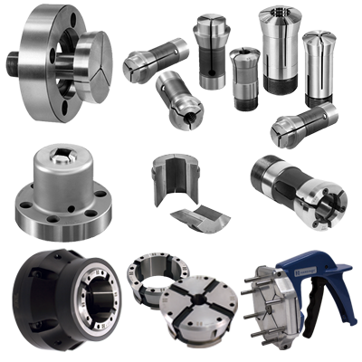
Hardinge is a leading global provider of advanced, high precision CNC Machine Tools’ solutions and aftermarket tooling and accessories.
With over 130 years of experience, the company has been a leader of innovation with a full spectrum of CNC turning, milling and grinding machines, and work holding products, providing customers and partners in over 50 countries worldwide with intelligent solutions for the world’s most demanding manufacturing requirements.
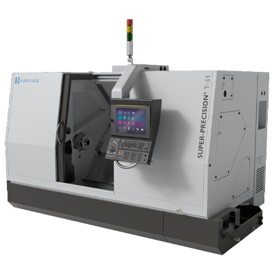
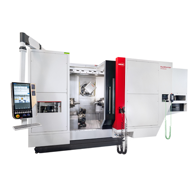
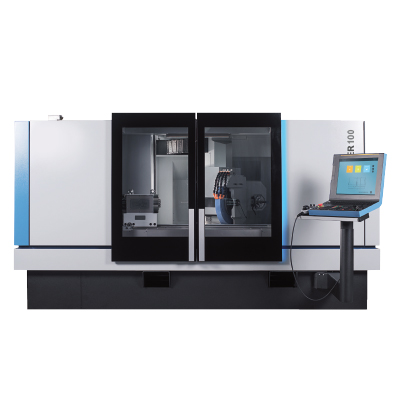
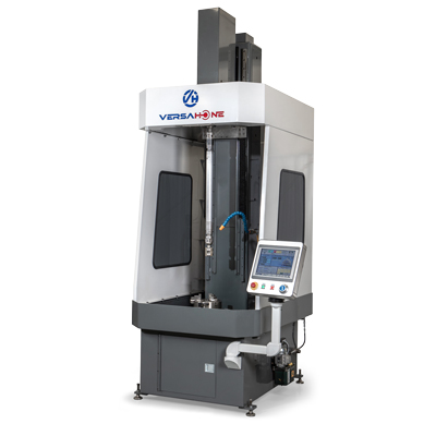
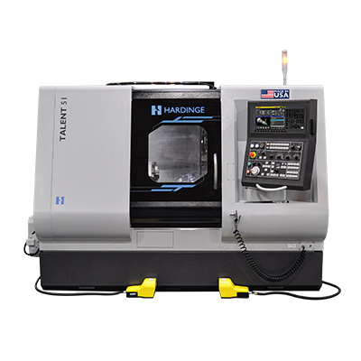
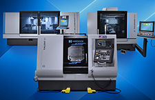
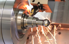
Our CNC machines provide proven technology with the ability to handle the world’s most challenging materials and the most complex machining geometries. We have extensive knowledge in building multi-tasking CNC grinders and integrated solutions to grind, mill and drill components such as boules, wafers, silicon electrodes, rings, chucks, and domes made from advanced ceramic materials.
These materials include single or multicrystal silicon (Si), alumina (Al2 3O ), aluminum nitride (AlN), silicon nitride (Si 3 4N ), silicon carbide (SiC), quartz glass (SiO2), GaN and ferrites.
Hardinge has a specialized team that focuses on innovative solutions for machining boules and wafers and advanced ceramics used in semiconductor processing machines. This team supplies clients with state-of-the-art multi-tasking CNC grinders and CNC precision lathes with up to 70%cycle time reductions, 45% of scrap reduction, machine uptimes above 95%, a reduced number of operators and a small footprint.
How does Hardinge support the latest manufacturing trends?
To be successful in the semiconductor market, Hardinge has combined the latest CNC control, measurement, mechanical and machining technology into one platform.
By increasing functionality, Hardinge can develop automated processes in single setups, combining different types of grinding. This allows customers to achieve higher productivity, surface finishes and consistent part quality when working with the most demanding materials.
To support the latest manufacturing trends, Hardinge solutions are integrated with smart technology and intelligent monitoring systems that are ideal for IoT and industry 4.0. Manufacturers can expect streamlined production processes when utilizing these platforms, leading to improved efficiency and productivity for machining advanced ceramics in the semiconductor industry.
Can you give specific examples of how Hardinge builds machines with extremely high utilization?
Hardinge offers a high resolution vision system for complex automatic part orienting, which focuses on the creation of new part centerline based on existing part features and allows an eccentric machining process to achieve concentricity based on the new centerline found.
We also offer laser measuring technologies for all the wheels in a tool changer and large OD wheels with automatic offset capabilities that compensate for the wear of a diamond dressing wheel. Furthermore, next-generation high-speed, high-accuracy lasers are effective for fast part setup and machining process control.
Hardinge provides high-resolution probing, measurement and feedback systems for automated machining to measure critical workpiece characteristics in-cycle, including automatic size correction capabilities.
We help clients achieve process control with closed-loop feedback using the probes’ data to update offsets directly on machine tool controls in a repeatable and reliable fashion, compensating for common causes of process instability.
Probing is the best way to maximize the manufacturing process’s efficiency, quality, capability, and accuracy. Standard routines in our modern CNC control simplify the integration of probing cycles into machining operations and offline tools. These routines, combined with a CAD interface, make simulation of measurement functions easy.
Our fully integrated 5-axis control architecture can achieve all grinding operations under optimal peripheral approach angles, including the ability to generate radii using straight wheels, thus achieving elevated surface finishes over the entire part.
Our industry-leading hydrostatic B/B1 axes swiveling technology can be applied to both workhead and wheelhead side for enhanced machine flexibility and is designed to support fully integrated 5-Axis control architecture to achieve all operations under optimal grinding conditions.
We also provide multi-spindle technology on same machine platform. This industry-leading solution allows users to select powerful lower speed spindles that are ideally suited for OD/face grinding operations using larger wheels while supporting high-speed spindles to optimize the processing of smaller features without compromising on performance.
Our automatic tool change spindle for speeds of up to 30,000 rpm is mounted on the vertical Y axis to complete off-center features in a very efficient manner. For the ATC spindle, we offer an integrated 20-position tool changer. We also provide a flexible wheel dressing with the rotary dresser attached to the workhead axis.
Finally, machine diagnostics, machine performance measurement and preventative maintenance is essential to establish a known and repeatable level of process capability. Our laser interferometer and ball bar measurement systems assess, monitor, and improve our CNC machine tools’ static and dynamic performance.
How does Hardinge builds CNC machines to meet the latest demands?
Hardinge has built many CNC lathes, CNC Vertical Machining Centers and CNC Grinders that are already running 24/7 in the semiconductor industry across different parts of the country. The current demand is developing CNC machines with multi-tasking capabilities to produce semiconductor parts in one setup, with faster production times and reduced waste.
How much revenue does Hardinge plan to earn from the semiconductor sector?
A primary objective of Hardinge is to become the number one CNC Machine supplier in the advanced ceramic manufacturing market. We also aim to develop, design, and manufacture state-of-the-art made-in-the-USA machines, taking them to the market and developing new machining technologies that can handle the world’s most challenging materials and the most complex machining geometries.
About Dr. Osman Boydas
Dr. Osman Boydas has over 35 years of sales and service experience in the CNC Machine Tools business, which has included hands-on experience in the design and production of parts for semiconductor, aerospace, defence, energy and medical industries. He holds PhDs in Engineering from MIT and WPI, along with a European patent for a fully automated welding machine. Additionally, he has written books and articles on grinding and metal cutting.
Source: AZoM.com

